 The IEEE International Electron Devices Meeting (IEDM) – the leading forum for the presentation of advances in microelectronic, nanoelectronic and bioelectronic devices – will celebrate its 60th anniversary when it gets underway next week in San Francisco.
"The IEDM conference has long been the place where the world's experts have presented breakthroughs in transistors, memory devices and related semiconductor technologies," said Suman Datta, IEDM 2014 publicity chair and Professor of Electrical Engineering at Penn State University. "The tradition of attracting the best speakers and a large, diverse audience from around the world continues as we mark the conference's 60th anniversary, with an added focus on emerging areas of importance where semiconductor technology is expected to play an expanding and enabling role."
More than 200 papers will be presented, including two particularly interesting pieces of research by IBM and the Japanese LEAP project.
The IBM paper addresses the challenge of creating FinFETs on advanced processes. According to the research team, high density fin formation is one of the most critical processes in the FinFET device fabrication flow. Because each fin in the device must be nearly identical, any new process must be able to form fins with a high degree of structural precision.
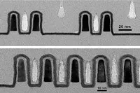
IBM's researchers are looking at directed self assembly using block copolymers (BCP) and 193nm immersion lithography to make FinFETs for beyond the 10nm node. The team has created a topographic template pattern in which the BCP is confined between the sidewalls of the template, driving the pattern into registry with the surface topography. Fins created at a pitch of 29nm are said to show good uniformity, with no signs of gross variation in critical dimensions.
The image shows, at the top, groups of two fins formed by the process, while, at the bottom, is a cross section of a larger group of fins.
Meanwhile, work continues to develop memory technologies which will support advanced manufacturing processes. There has been much research into phase change memory, in which a chalcogenide is shifted between its crystalline and amorphous states to represent a 0 or a 1. However, a team from LEAP – the Low Power Electronics Association and Project – believes it has created a superior approach, which it calls topological switching RAM, or TRAM
In this approach, data is stored according to the movement of Ge atoms in a GeTe/Sb2Te3 crystal superlattice. TRAM is said to require up to 20 times less programming energy than a chalcogenide based approach.
Author
Graham Pitcher
Source: www.newelectronics.co.uk
