Electronics News
Archive : 23 January 2015 год
 IT researchers working at the University of Twente say they have developed a programming language which could make the cost of designing hardware more manageable.
For the last 20 years, chip manufacturers have been using the same chip design techniques in which extensive testing is required after each design step. The newly developed functional programming language should, say the researchers, make it possible to prove, in advance, that a design transformation is a 100% error free.
"While a software developer can fix a programming error by developing and distributing a patch, a single flaw in chip design means that all products containing the chip need to be recalled," said doctoral candidate Christiaan Baaij.
"Clearly, the design process requires extensive and repeated testing. Such testing is expensive, but is still absolutely necessary. A company like NVidia nowadays incurs more than $1billion in design expenses annually."
Functional programming languages are said to allow the user to formally prove the correctness of design transformations. Because functional verification can prove that transformations do not alter the chip's behaviour, it is not necessary to verify and reverify each step of the design process. In turn, says Baaij, this means the complexity – and the cost – of chip design can be managed more readily.
One important element of this research involves the C?aSH compiler, which transforms hardware descriptions written in the Haskell functional language into a lower level description. Standard software can then create a chip from this description. Baaij's work concerns the development of this compiler, allowing for the automatic generation of the hardware from an abstract description.
Author
Graham Pitcher
Source: www.newelectronics.co.uk
 Although graphene based devices have shown outstanding electrical and optical performance, they are sensitive to environmental factors, such as humidity or gas composition. This, says a research team, has made reproducible operation in a normal atmosphere impossible.
Generally, adsorbates from the ambient (such as moisture or oxygen) and residuals from lithography processes, adhere to the graphene and change its doping level unintentionally. As these contaminants are unstable under normal conditions, the doping level – and hence the electrical and optical properties – also change. The variation in these parameters is said by the team to be a major roadblock for using graphene devices in applications.
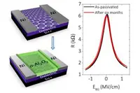
However, the researchers – from AMO and Graphenea – have developed an encapsulation technique that enables graphene devices to demonstrate reproducible operation in a normal atmosphere for several months.
The researchers encapsulated graphene field effect devices using aluminum oxide, an encapsulation material applied in OLEDs. The key parameter for device passivation found in this study is the growth of an oxide layer using a properly in situ oxidised aluminum seed layer. This passivation layer can stabilise device characteristics over several months when stored and measured in ambient atmosphere. This, the team concludes, is a major step towards the use of graphene devices in real applications.
Author
Graham Pitcher
Source: www.newelectronics.co.uk
