Electronics News
Archive : 9 January 2015 год
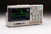
 Keysight Technologies has introduced a digital-storage and mixed signal oscilloscope with an intuitive graphical triggering capability. The InfiniiVision 3000T X-Series promises to deliver capacitive touch screens and zone triggering to the mainstream oscilloscope market for the first time to help engineers overcome the historical difficulties of usability and triggering.
As digital speeds and device complexity continue to increase, signals under test are getting more complex and isolating anomalies in devices is becoming more of a challenge. Intuitive graphical triggers, previously unavailable in mainstream oscilloscopes, help engineers debug and characterise their cutting-edge devices faster and more easily. With graphical triggers, engineers can use a finger to draw a box around a signal of interest on the instrument display to create the necessary trigger.
The new oscilloscope series offers upgradable bandwidths from 100 MHz to 1.0 GHz. This uncompromised update rate of one million waveforms per second gives engineers visibility into very subtle signal details.
The series comes with six-instruments-in-one integration, including oscilloscope functionality, digital channels (MSO), protocol analysis capability, a digital voltmeter, a WaveGen function/arbitrary waveform generator, and an 8-digit hardware counter/'totalizer'.
The 3000T X-Series also correlates frequency and time domain measurements using the gated FFT function for the first time in its class, to address emerging measurement challenges.
Dave Cipriani, vice president and general manager of Keysight's Oscilloscope and Protocol Division, said: "These new scopes give engineers using mainstream oscilloscopes an uncompromised ability to find and isolate the most difficult problems in their designs. Design-for-touch operation improves their debugging efficiency. Mixed-domain analysis capabilities with time-correlated frequency/time domain measurements, six-in-one integration and a rich set of advanced features accelerate their problem solving."
Author
Justin Cunningham
Source: www.newelectronics.co.uk
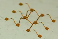
 Researchers at the University of Illinois at Urbana-Champaign have developed a process for geometrically transforming 2D micro/nanostructures into extended 3D layouts.
"Conventional 3D printing technologies are fantastic," said Professor John Rogers, "but none offers the ability to build microstructures that embed high performance semiconductors. We have presented a remarkably simple route to 3D that starts with planar precursor structures formed in nearly any type of material, including the most advanced ones used in photonics and electronics.
"A stretched, soft substrate imparts forces at precisely defined locations across such a structure to initiate controlled buckling processes that induce rapid, large-area extension into the third dimension. The result transforms these planar materials into well-defined, 3D frameworks with broad geometric diversity."
Initial demonstrations are said to include experimental and theoretical studies of more than 40 geometries, ranging from single and multiple helices to structures that resemble spherical baskets, as well as scaffolds, fences and frameworks, each with single and/or multiple level configurations, constructed in various materials, including semiconductors, conductors and dielectrics.
"We're now exploiting these ideas in the construction of high performance electronic scaffolds for actively guiding and monitoring growth of tissue cultures and networks for 3D electronic systems that can bend and shape themselves to the organs of the human body. We're very enthusiastic about the possibilities," Prof Rogers concluded.
Author
Graham Pitcher
Source: www.newelectronics.co.uk
