Electronics News
Archive : 9 November 2014 год
 The MEMS Industry Group (MIG) has announced the Accelerated Innovation Community (AIC), an open source algorithm cooperative intended to collaboration across the MEMS/sensors supply chain.
MIG executive director Karen Lightman said: "When companies are developing products that use MEMS/sensors, they often have to develop algorithms from scratch. This inhibits innovation by compelling designers to reinvent the wheel on common algorithms every time they want to add or change functionality in their product. Giving them access to an open-source library of introductory algorithms fundamentally changes the development paradigm. Product designers can use field-proven, open-source algorithms supplied by MIG member companies to jumpstart their development process, enabling them to gain all the benefits of MEMS/sensors that much faster."
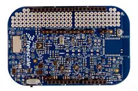
One of the first companies to support the initiative is Freescale, which contributing sensor fusion software, as well as its sensor fusion development kit and additional development technology based on the Freedom development platform (pictured).
"Sensor fusion is a fundamental building block for today's secure embedded processing solutions. Although it has been in the market for several years, sensor fusion has so far been kept proprietary, and this has unnecessarily slowed its broader adoption," said Babak Taheri, general manager of Freescale's sensor solutions division. "With our comprehensive development tools and support for AIC's open source initiative, Freescale will help even more developers and systems designers unleash the benefits of sensor fusion technology, ultimately leading to the creation of compelling new IoT products and services."
Other supporters of AIC include Analog Devices and Carnegie Mellon University, with more MIG members expected to contribute to the inititiative in the near future.
Author
Graham Pitcher
Source: www.newelectronics.co.uk
 Researchers in the UK have found a way to manipulate glass to create a material that allows computers to transfer information using light – a development which could significantly increase computer processing speeds.
A team led by the University of Surrey, in collaboration with the Universities of Cambridge and Southampton, found a way to change the electronic properties of amorphous chalcogenides, a glass material integral to data technologies such as CDs and DVDs.
By using a technique called ion doping, they discovered they could use light to bring together different computing functions into one component, leading to all-optical systems.
Computers currently use electrons to transfer information and process applications. Data sources such as the internet, however, rely on optical systems; the transfer of information using light.
Optical fibres are used to send information around the world at the speed of light, but these signals then have to be converted to electrical signals once they reach a computer, causing a significant slowdown in processing.
"The challenge is to find a single material that can effectively use and control light to carry information around a computer," explained project leader Dr Richard Curry, of the University of Surrey. "Much like how the web uses light to deliver information, we want to use light to both deliver and process computer data."
Dr Curry continued: "This has eluded researchers for decades, but now we have now shown how a widely used glass can be manipulated to conduct negative electrons, as well as positive charges, creating what are known as 'pn-junction' devices. This should enable the material to act as a light source, a light guide and a light detector – something that can carry and interpret optical information. In doing so, this could transform the computers of tomorrow, allowing them to effectively process information at much faster speeds."
The team believes the results of the research will be integrated into computers within ten years. In the short term, the glass is already being developed and used in next generation computer memory technology known as CRAM.
Author
Laura Hopperton
Source: www.newelectronics.co.uk
 Invecas, a newly formed design services provider, has signed a deal under which it will provide exclusive support for Globalfoundries' customers. The partnership is intended to support companies of various sizes operating in a range of markets who are looking to differentiate their products through customised silicon.
Invecas will focus on offering design services for Globalfoundries' leading edge processes, including 14nm FinFET. It will operate design service centres in the US and India, staffed by more than 600 engineers.
"These newly launched centres will provide a significant complement to our in house global design solutions capabilities while enhancing our existing ecosystem of design and IP partners," said Gregg Bartlett, Globalfoundries' senior vice president of product management. "The Invecas team has a strong track record of providing spec-to-silicon solutions for complex SoCs in multiple high-volume market segments. It will be an excellent partner to help us expand the services available to customers designing products on the leading edge of technology."
Through Invecas, customers will have access to services such as system design, embedded software design, SoC design and verification and physical implementation.
"By combining our system level expertise with a focus on Globalfoundries' advanced processes, Invecas brings unrivalled expertise to some of the most difficult issues facing designers today," said chairman Dasaradha Gude. "This will enable a broader range of customers to accelerate time-to-volume of designs on complex technologies like 14nm FinFETs."
Invecas will also offer a selection of design IP across various Globalfoundries process nodes, include standard cells, I/O, memories, analogue and complex interface IP solutions.
Author
Graham Pitcher
Source: www.newelectronics.co.uk
